
Chapter 6 Solids And Semiconductors Devices Multiple Choice Questions Exercise -1 Section (A) Semiconductor, Energy Band
Question 1. A N-type semiconductor is
- Negatively charged
- Positively charged
- Neutral
- None of these
Answer: 3. Neutral
Question 2. The forbidden energy band gap in conductors semiconductors and insulators are EG1, EG2, and EG3 respectively, The relation among them is
- EG1 = EG2 = EG3
- EG1 < EG2 < EG3
- EG1 > EG2 > EG3
- EG1 < EG2 > EG3
Answer: 2. EG31 < EG2 < EG3
Question 3. The mobility of free electrons is greater than that of free holes because
- They carry a negative charge
- They are light
- They mutually collide less
- They require low energy to continue their motion
Answer: 4. They require low energy to continue their motion
Question 4. Electric conduction in a semiconductor takes place due to
- Electrons Only
- Holes Only
- Both Electrons And Holes
- Neither electrons nor Holes
Answer: 3. Both Electrons And Holes
Solids and Semiconductor Devices MCQs for NEET Physics Class 12
Question 5. Let n p and n e be the numbers of holes and conduction electrons in an intrinsic semiconductor
- np > ne
- np = ne
- np < ne
- np ≠ ne
Answer: 2. np = ne
Question 6. Let np and ne be the numbers of holes and conduction electrons in an extrinsic semiconductor
- np > ne
- np = ne
- np < ne
- np ≠ ne
Answer: 4. np ≠ ne
Question 7. An electric field is applied to a semiconductor. Let the number of charge carriers be n and the average drift speed be. If the temperature is increased,
- Both N And υ Will Increase
- N Will Increase But υ Will Decrease
- υ Will Increases But N Will Decrease
- Both N And υ Will Decrease
Answer: 2. N Will Increase But υ Will Decrease
Question 8. When an impurity is doped into an intrinsic semiconductor, the conductivity of the semiconductor
- Increases
- Decreases
- Remains The Same
- Become Zero
Answer: 1. Increases
Question 9. In a P-type semiconductor, the acceptor level is 57 meV, above the valence band. The maximum wavelength of light required to produce a hole will be
- 57 A°
- 57 × 10¯³ A°
- 217100 A°
- 11.61 × 10 A°
Answer: 3. 217100 A°
Question 10. The electrical conductivity of pure germanium can be increased by
- Increasing The Temperature
- Doping Acceptor Impurities
- Doping Donor Impurities
- Irradiating Ultraviolet Light On It.
Answer: 1. Increassing The Temperature
Question 11. A semiconductor is doped with a donor impurity
- The hole concentration increases
- The hole concentration decreases
- The electron concentration increases
- The electron concentration decreases
Answer: 2. The hole concentration decreases
Question 12. Which of the following when added as an impurity into silicon produces an n-type semiconductor?
- P
- Al
- B
- Mg
Answer: 1. P
Question 13. Which of the following diagrams correctly represents the energy levels in the p-type semiconductor?

Question 14. In p-type semiconductor, the major charge carriers are :
- Holes
- Electrons
- Protons
- Neutrons
Answer: 3. Protons
Question 15. Copper and silicon are cooled from 300 K to 60K, and the specific resistance:-
- Decrease in copper but an increase in silicon
- Increase in copper but an increase in silicon
- Increase in both
- Decrease in both
Answer: 1. Decrease in copper but increase in silicon
Question 16. The value of the forbidden energy gap for the conductor is:
- 1 eV
- 6 eV
- 0 eV
- 3 eV
Answer: 1. 1 eV
Question 17. Ga As is a /an :
- Element Semiconductor
- Alloy Semiconductor
- Bad Conductor
- Metalic Semiconductor
Answer: Alloy Semiconductor
Question 18. The number of free electrons in Si at normal temperature is :
- 2.5 × 10⁶ per cm3
- 1.5 × 10¹⁰ per cm3
- 1.5 × 10¹³ per cm3
- 2.5 × 10¹³ per cm3
Answer: 2. 1.5 × 10¹⁰ per cm3
Question 19. Hole are the charge carriers in :
- Semiconductor
- Ionic Solids
- P-Type Semiconductor
- Metals
Answer: 1. Semiconductor
Question 20. Regarding a semi-conductor which one of the following is wrong?
- There are no free electrons at 0 K
- There are no free electrons at room temperature
- The number of free electrons increases with the rise in temperature
- The charge carriers are electrons and holes.
Answer: 2. There are no free electrons at room temperature
Question 21. At absolute zero, Si acts as :
- Non-Metal
- Metal
- Insulator
- None Of These
Answer: 3. Insulator
Question 22. By increasing the temperature, the specific resistance of a conductor and ~ semiconductor:
- Increases For Both
- Decreases For Both
- Increases, Decreases Respectively
- Decreases, Increases Respectively
Answer: 3. Increases, Decreases Respectively
Question 23. The energy band gap is maximum in:
- Metals
- Superconductors
- Insulators
- Semiconductors
Answer: 3. Insulators
Question 24. A strip of copper and another of germanium are cooled from room temperature to 80 K. The resistance of :
- Each Of These Decreases
- Copper Strip Increases And That Of Germanium Decreases
- Copper Strip Decreases And That Of Germanium Increases
- Each Of These Increases
Answer: 3. Copper Strip Decreases And That Of Germanium Increases
Question 25. The difference in the variation of resistance with temperature in a metal and a semiconductor arises essentially due to the difference in the:
- Crystal Structure
- Variation Of The Number Of Charges Carries With Temperature
- Type Of Bonding
- Variation Of Scattering Mechanism With Temperature
Answer: 2. Variation Of The Number Of Charges Carries With Temperature
Question 26. In p-type semiconductors germanium is doped with :
- Gallium
- Aluminium
- Boron
- All Of These
Answer: 4. All Of These
Question 27. In a good conductor of electricity, the type of bonding that exists is :
- Ionic
- Van Der Waal
- Covalent
- Metallic
Answer: 4. Metallic
Question 28. Which of the following statements is true for an n-type semiconductor?
- The donor level lies closely below the bottom of the conduction band
- The donor level lies closely above the top of the valence band
- The donor level lies at the halfway mark of the forbidden energy gap
- None of the above
Answer: 1. The donor level lies closely below the bottom of the conduction band
Question 29. An n-type semiconductor is
- Negatively Charged
- Positively Charged
- Neutral
- None Of The Above
Answer: 3. Neutral
Question 30. The difference in the variation of resistance with temperature in a metal and a semiconductor arises essentially due to the difference in the
- Crystal Structure
- Change In The Number Of Charge Career
- Type Of Bonding
- None Of These
Answer: 2. Change In The Number Of Charge Career
Question 31. In P-Type Semiconductors Majority Charge Carriers Are
- Electrons
- Holes
- Neutrons
- Protons
Answer: 2. Holes
Question 32. Wire P and Q have the same resistance at ordinary (room) temperature. When heated, the resistance of P increases, and that of Q decreases. we conclude that
- p and Q are conductors of different materials.
- p is an n-type semiconductor and Q is a p-type semiconductor
- p is semiconductor and Q is conductor
- p is conductor and Q is semiconductor
Answer: 4. p is a conductor and Q is a semiconductor
Question 33. The resistance of a semiconductor and a conductor:
- Increases With Temperature For Both
- Decreases With Temperature For Both
- Increases And Decreases Respectively With Increase In Temperature
- Decreases And Increases Respectively With Increase In Temperature
Answer: 4. Decreases And Increases Respectively With Increase In Temperature
Question 34. In semiconductors at room temperature
- The valence band is filled and the conduction band is partially filled
- The valence band is filled
- The conduction band is empty
- The valence band is partially empty and the conduction band is partially filled
Answer: 4. The valence band is partially empty and the conduction band is partially filled
Question 35. Carbon, Silicon, and Germanium atoms have four valence electrons each. Their valence and conduction bonds are separated by energy band gaps represented by (Eg ) C, (Eg)si, and (Eg) Ge respectively. Which one of the following relationships is true in their case
- (Eg)c < (Eg)Ge
- (Eg)c > (Eg)si
- (Eg)c = (Eg)si
- (Eg)c < (Eg)si
Answer: 2. (Eg)c > (Eg)si
Question 36. In the energy band diagram of a material shown below, the open circles and filled circles denote holes and electrons respectively. The material is a/an :
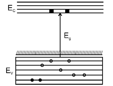
- P-Type Semiconductor
- Insulator
- Metal
- N-Type Semiconductor
Answer: 1. P-Type Semiconductor
Question 35. Choose the correct option for the forward-biased characteristics of a p–n junction.

Answer: 3.
Question 36. The emitter-base junction of a transistor is …….biased while the collector-base junction is …….biased
- Reverse, forward
- Reverse, reverse
- Forward, forward
- Forward, reverse
Answer: 4. Forward, reverse
Question 37. If the two ends of a P-N junction are joined by a wire-
- There will not be a steady current in the circuit
- There will be a steady current from the N-side to the P-side
- There will be a steady current from the P-side to the N-side
- There may or may not be a current depending upon the resistance of the connecting wire.
Answer: 1. There will not be a steady current in the circuit
Question 38. The region that has no free electrons and holes in a P-N juction is-
- P-region
- N-region
- Junction
- Depletion Region
Answer: 4. Depletion Region
Question 39. In the P-N junction at the near junction, there are-
- Only Positive Ions
- Only Negative Ions
- Positive And Negative Ion Both
- Electron And Holes Both
Answer: 3. Positive And Negative Ion Both
Class 12 NEET Physics Solids and Semiconductor Devices MCQs
Question 40. A diode is made forward biased by a two-volt battery however there is a drop of 0.5 V across the diode which is independent of the current. Also, a current greater than 10 mA produces large joule loss and damages the diode. If the diode is to be operated at 5 mA, the series resistance to be put is-

- 3 KΩ
- 300 KΩ
- 300Ω
- 200 KΩ
Answer: 3. 300Ω
Question 41. The ratio of resistance for forward to reverse bias of the P–N junction diode is-
- 10²: 1
- 10–²: 1
- 1: 10–4
- 1: 10
Answer: 4. 1: 10
Question 42. Zener diode is used-
- As an amplifier
- As a rectifier
- As an oscillator
- As a voltage regulator
Answer: 2. As a rectifier
Question 43. The zener breakdown will occur if-
- The impurity level is low
- The impurity level is high
- Impurity is less on the N-side
- Impurity is less on P-side
Answer: 2. Impurity level is high
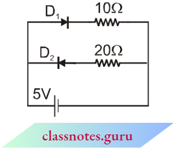
Question 44. In the given fig. which of the diodes are forward-biased

- 1,2,3
- 2,4,5
- 1,3,4
- 2,3,4
Answer: 1. 1,2,3
Question 45. Consider the following statements A and B and identify the correct answer-
- A zener diode is always connected in reverse bias.
- The potential barrier of a P-N junction lies between 0.1 to 0.3 V approximately.
Choose The Correct Answer
- A and B are correct
- A and B are wrong
- A is correct, but B is wrong
- A is wrong, but B is correct
Answer: 3. A is correct, but B is wrong
Question 46. The function of the rectifier is
- To convert AC into DC
- To convert dc into ac
- Both and
- None of these
Answer: 1. To convert AC into dc
Question 47. The cause of the potential barrier in a p-n diode is:
- Depletion Of Positive Charges Near The Junction
- Concentration Of Positive Charges Near The Junction
- Depletion Of Negative Charges Near The Junction
- Concentration Of Positive And Negative Charges Near The Junction
Answer: 4. Concentration Of Positive And Negative Charges Near The Junction
Question 48. A semi-conducting device is connected in a series in a circuit with a battery and a resistance. A current is allowed to pass through the circuit. If the polarity of the battery is reversed, the current drops to almost zero. The device may be:
- A P-N Junction
- An Intrinsic Semiconductor
- A P-Type Semiconductor
- An N-Type Semiconductor
Answer: 1. A P-N Junction
Question 49. In a junction diode, the holes are due to:
- Protons
- Extra Electrons
- Neutrons
- Missing Electrons
Answer: 4. Missing Electrons
Question 50. The depletion layer consists of:
- Electrons
- Protons
- Mobile Charge Carriers
- Immobile Ions
Answer: 4. Immobile Ions
Question 51. In forward bias the width of the depletion layer in a p-n junction diode:
- Increases
- Decreases
- Remains Constant
- First Increases Then Decreases
Answer: 2. Decreases
Question 52. The current (I) in the circuit will be

- \(\frac{5}{40} \mathrm{~A}\)
- \(\frac{5}{50} \mathrm{~A}\)
- \(\frac{5}{10} \mathrm{~A}\)
- \(\frac{5}{20} \mathrm{~A}\)
Answer: 2. \(\frac{5}{50} \mathrm{~A}\)
Question 53. In a P-N junction diode not connected to any circuit-
- High potential at the N side and low potential at the P side
- High potential at the P side and low potential at the N side
- P and N both have at same potential
- The potentials of the N side and P side are undetermined
Answer: 1. High potential at the N side and low potential at the P side
Question 54. In a PN junction:-
- High potential at the N side and low potential at the P side
- High potential at the N side and low potential at the N side
- P and N both have at same potential
- Undetermined
Answer: 1. High potential at the N side and low potential at the P side
Question 55. Reverse bias applied to a junction diode-
- Lowers the potential barrier
- Raises the potential barrier
- Increases the majority carrier’s current
- Decreases the minority carrier’s current
Answer: 2. Raises the potential barrier
Question 56. The barrier potential of a p-n junction diode does not depend on-
- Diode design
- Temperature
- Forward bias
- Doping density
Answer: 1. Diode design
Question 57. The inverse saturation current in a P-N junction diode at 27°C is 10–5 amp. The value of forward current at 0.2 volts will be (e7.62 = 2038.6)
- 2037.6 × 10–3 A
- 203.76 × 10⁻³ A
- 20.376 × 10⁻³ A
- 2.0376 × 10⁻³ A
Answer: 3. 20.376 × 10⁻³ A
Question 58. The reason for the potential barrier in the p-n junction is:
- Excess Of Positive Charge At Junction
- Deficiency Of Positive Charge At Junction
- Deficiency Of Negative Charge At Junction
- Excess Of Positive And Negative Charge At Junction
Answer: 4. Excess Of Positive And Negative Charge At Junction
Question 59. In p-n junction depletion region decreases when:
- Zero Bias
- Forward Bias
- Reverse Bias
- Temperature Decreases
Answer: 2. Forward Bias
Question 60. Two identical P-N junctions may be connected in series with a battery in three ways (fig below). The potential drops across the two P-N junctions are equal in

- Circuits 1 and 2
- Circuits 2 and 3
- Circuit 3 and 1
- Circuit 1 only
Answer: 3. Circuit 3 and 1
Question 62. In a P-N junction diode which is not connected to any circuit-
- The potential is the same everywhere
- The P-type side is at a higher potential than the N-type side
- There is an electric field at the junction directed from the N-type side to the P-type side
- There is an electric field at the junction directed from the P-type side to the N-type side
Answer: 2. The P-type side is at a higher potential than the N-type side
Question 63. For the given circuit shown in Fig, to act as a full wave rectifier, a.c. input should be connected across ……..and……..the d.c. output would appear across……..and……..

- A, C and B, D
- B, D and A, C
- A, B C, D
- C, A and D, B
Answer: 3. A, B C, D
Question 64. In a……biased P-N junction the net flow holes is from the N-region to the P-region-
- Forward Bias
- Reverse Bias
- no
- Both 1 and 2
Answer: 2. Reverse Bias
Question 65. For making the p-n junction diode forward biased:
- The same Potential Is Applied
- Greater Potential Is Given To N Compared To P
- Greater Potential Is Given To P Compared To N
- Unbalanced Concentration
Answer: 3. Greater Potential Is Given To P Compared To N
Question 66. When a p-n junction diode is reverse-biased, then
- No Current Flows
- The Depletion Region Is Increased
- The Depletion Region Is Reduced
- The Height Of The Potential Barrier Is Reduced
Answer: 2. The Depletion Region Is Increased
Question 67. In the middle of the depletion layer of reverse biased p – n juction, the
- Electric Field Is Zero
- Potential Is Maximum
- The Electric Field Is the Maximum
- Potential Is Zero
Answer: Electric Field Is Zero
Question 68. If the input is given between A and C, then the output at the ends of R will be

- Fully Rectified
- Half Rectified
- Ac
- None Of These
Answer: 2. Half Rectified
Question 69. Of the diodes shown in the following diagrams, which one of the diodes is reverse biased?


Answer: 2.
Question 70. Application of a forward bias to a p-n junction –
- Widens the depletion zone
- Increases the number of donors on the N-side
- Increases the potential difference across the depletion zone
- Increases the electric field in the depletion zone
Answer: 4. Increases the electric field in the depletion zone
Question 71. A forward-biased diode is:-

Answer: 4.
Question 72. A p-n photodiode is made of a material with a band gap of 2.0 eV. The minimum frequency of the radiation that can be absorbed by the material is nearly
- 10 × 1014 Hz
- 5 × 10¹⁴ Hz
- 1 × 10¹⁴ Hz
- 20 × 1014 Hz
Answer: 2. 5 × 10¹⁴ Hz
Question 73. When the P-N junction diode is forward-biased, then-
- The Depletion Region Is Reduced And Barrier Height Is Increased.
- The Depletion Region Is Widened And the Barrier Height Is Reduced.
- Both The Depletion Region And Barrier Height Are Reduced.
- Both The Depletion Region And Barrier Height Are Increased.
Answer: 3. Both The Depletion Region And Barrier Height Are Reduced.
Question 74. In a full wave rectifier circuit operating from 50 Hz mains frequency, the fundamental frequency in the ripple would be:
- 50Hz
- 25Hz
- 100Hz
- 70.7Hz
Answer: 3. 100Hz
Question 75. In the following, which one of the diodes is reverse-biased?

Answer: 2.
Question 76. The circuit has two oppositely connected ideal diodes in parallel. What is the current flowing in the circuit?
- 2.31A
- 1.33A
- 1.71A
- 2.00A
Answer: 4. 2.00A
Question 77. The drift current in a p-n junction is
- From The N-Side To The P-Side
- From The P-Side To The N-Side
- From The N-Side To The P-Side If The Junction Is Forward-Baised And In The Opposite Direction If It Is Reverse-Biased
- From The P-Side To The N-Side If The Junction Is Forward-Biased And In The Opposite Direction If It Is Reverse-Baised
Answer: 1. From The N-Side To The P-Side
NEET Physics Class 12 Chapter 6 MCQs on Solids and Semiconductors
Question 78. The diffusion current in a p-n junction is
- From The N-Side To The P-Side
- From The P-Side To The N-Side
- From The N-Side To The P-Side Of The Junction Is Forward-Biased And In The opposite direction If It Is Reverse-Baised
- From The P-Side To The N-Side If The Junction Is Forward-Baised And In The Opposite Direction If It Is Reverse-Biased
Answer: 2. From The P-Side To The N-Side
Question 79. A semiconducting device is connected in a series circuit with a battery and a resistance. A current is found to pass through the circuit. If the polarity of the battery is reversed, the current drops to almost zero. The device may be
- An Intrinsic Semiconductor
- A P-Type Semiconductor
- An N-Type Semiconductor
- A P-N Junction
Answer: 4. A P-N Junction
Question 80. If the two ends P and N of a P-N of a P-N diode junction are joined by a wire
- There will not be a steady current in the circuit
- There will be a steady current from the N side to the P side
- There will be a steady current from the P side to the N side
- There may not be a current depending upon the resistance of the connecting wire
Answer: 1. There will not be a steady current in the circuit
Question 81. To make a PN junction conducting
- The value of forward bias should be more than the barrier potential
- The value of forward bias should be less than the barrier potential
- The value of reverse bias should be more than the barrier potential
- The value of reverse bias should be less than the barrier potential
Answer: 1. The value of forward bias should be more than the barrier potential
Question 82. Zener diode is used as
- Half Wave Rectifier
- Full Wave Rectifier
- Ac Voltage Stabilizer
- Dc Voltage Stabilizer
Answer: 3. Ac Voltage Stabilizer
Question 83. In the P-N junction, the barrier potential offers resistance to
- Free electrons in the N region and holes in the P region
- Free electrons in the P region and holes in the N region
- Only free electrons in the N region
- Only holes in the P region
Answer: 1. Free electrons in the N region and holes in the P region
Question 84. Two identical P-N diodes are connected in series in the following ways. Maximum current will flow in a circuit
- A
- B
- C
- D
Answer: 2. B
Question 85. In the following circuit readings in ammeters A1 and A2 will be
- 0.2A, Zero
- Xero, o.2 A
- 0.2A, 0.2A
- 0.2A,0.4A
Answer: 2. Xero, o.2 A
Question 86. A light-emitting diode has a voltage drop of 2 v across it and passes a current of 10 A. When it operates with a 6 v battery through a limiting resistor R, the value of R is
- 40 kΩ
- 4 kΩ
- 200 kΩ
- 400 kΩ
Answer: 4. 400 kΩ
Chapter 6 Solids And Semiconductors Devices Multiple Choice Questions Section (C): Transistors
Question 1. An amplifier is nothing but an oscillator with –
- Positive Feedback
- High Gain
- No Feed Back
- Negative Feed Back
Answer: 1. Positive Feedback
Question 2. In A Normal Operation Of A Transistor,
- The Base-Emitter Junction Is Forward-Biased
- The Base-Collector Junction Is Forward-Biased
- The Base-Emitter Junction Is Reverse-Baised
- The Base-Collector Junction Is Reverse-Baised
Answer: 1. The Base-Emitter Junction Is Forward-Biased
Question 3. In the case of constants α and β of a transistor
- α = β
- β < 1 α > 1
- αβ = 1
- β > 1 α< 1
Answer: 4. β > 1 α< 1
Question 4. If α= 0.98 and current through emitter i e = 20 mA, the value of β is
- 4.9
- 49
- 96
- 9.6
Answer: 2. 49
Question 5. The transfer ratio B of a transistor is 50. the input resistance of the transistor when used in the common emitter configuration is 1 kΩ The peak value of the collector AC for an AC input voltage of 0.01 V peak is:
- 100 µA
- 0.01 mA
- 0.25 mA
- 500 µA
Answer: 4. 500 µA
Question 6. For a common emitter circuit if E I = 0.98 then the current gain for the common emitter circuit will be :
- 49
- 98
- 4.9
- 25.5
Answer: 1. 49
Question 7. A n-p-n transistor conducts when
- Both Collector And Emitter Are Positive Concerning The Base
- Collector Is Positive And Emitter Is Negative Concerning The Base
- Collector Is Positive And Emitter Is At the Same Potential As The Base
- Both Collector And Emitter Are Negative Concerning The Base
Answer: 2. Collector Is Positive And Emitter Is Negative Concerning The Base
Question 8. A Transistor (Pnp Or Npn) Can Be Used As
- An Amplifier
- An Oscillator
- A Switch
- All Of These
Answer: 4. All Of These
Question 9. The part of a transistor that is most heavily doped to produce a large number of majority charge carries is :
- Emitter
- Base
- Collector
- Can Be Any Of The Above Three
Answer: 1. Emitter
Question 10. In a common-base configuration of transistor. α = 0.98, I B = 0.02 mA, RL = 5 kΩ. The output voltage across the load is:

- 3.2 v
- 4.9v
- 5.2v
- 6.2v
Answer: 2. 4.9v
Question 11. The minimum potential difference between the base and emitter required to switch a silicon transistor ‘ON’ is approximately?
- 1 V
- 3 V
- 5 V
- 4.2 V
Answer: 1. 1 V
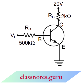
Question 12. In the circuit shown in the figure, the current gainβ= 100 for an npn transistor. The bias resistance RB so that V CE = 5V is (VBE << 10 V)
- 2 × 10³Ω
- 105Ω
- 2 × 10⁵Ω
- 5 × 10⁵Ω
Answer: 3. 2 × 10⁵Ω
Question 13. In a common emitter amplifier using an output resistance of 5000 ohms and input resistance of 2000 ohm, if the peak value of input signal voltage is 10 mV and β= 50 then the calculated power gain will be
- 6.25 × 10³
- 1.4
- 62.5
- 2.5 × 10
Answer: 1. 6.25 × 10³
Question 14. A transistor oscillator using a resonant circuit with an inductor L (of negligible resistance) and a capacitor C in series produces oscillations of frequency. If L is doubled and C is changed to 4C, the frequency will be:
- \(\frac{f}{4}\)
- 8f
- \(\frac{f}{2 \sqrt{2}}\)
- \(\frac{f}{2}\)
Answer: 3. \(\frac{f}{2 \sqrt{2}}\)
Question 15. A transistor is operated in a common emitter configuration at constant collector voltage Vc = 1.5 V such that a change in the base current from 100 µA to 150 µA produces a change in the collector current from 5 mA to 10 mA. The current gain (β) is:-
- 67
- 75
- 100
- 50
Answer: 3. 100
Question 16. A common emitter amplifier has a voltage gain of 50 and a current gain is 25. The power gain of the amplifier is:
- 500
- 1000
- 1250
- 100
Answer: 3. 1250
Question 17. When npn transistor is used as an amplifier:
- Electrons Move From Base To Collector
- Holes Move From Emitter To Base
- Electrons Move From Collector To Base
- Holes Move From Base To Emitter
Answer: 4. Holes Move From Base To Emitter
Question 18. In a common base amplifier, the phase difference between the input signal voltage and output voltage is :
- \(\frac{\pi}{4}\)
- Zero
- \(\frac{\pi}{2}\)
Answer: 3. Zero
Question 19. In a common–base mode of transistor, the collector current is 5.488 mA for an emitter current of 5.60 mA. The value of the base current amplification factor will be:
- 49
- 50
- 51
- 48
Answer: 1. 49
Question 20. A working transistor with its three legs marked P, Q, and R is tested using a multimeter. No conduction is found between P and Q. By connecting the common (negative) terminal of the multimeter to R and the other (positive) terminal to P or Q, some resistance is seen on the multimeter. Which of the following is true for the transistor?
- It is a PNP transistor with R as a collector
- It is a PNP transistor with R as an emitter
- It is an NPN transistor with R as a collector
- It is an NPN transistor with R as the base
Answer: 4. It is a PNP transistor with R as a collector
Question 21. An N-P-N transistor is connected in a common emitter configuration in which the collector supply is 9V and the voltage drop across the load resistance of 1000 connected in the collector circuit is 1 V. If the current amplification factor is (25/26), if the internal resistance of the transistor is 200, then which of the following options is incorrect amplification factor is (25/26), if the internal resistance of the transistor is 200, then which of the following options is incorrect

- \(V_{C E}=8 \mathrm{~V}\)
- The collector current is 1.0 mA
- Voltage gain \(\frac{50}{23}\) and power gain is 4.6
- The emitter current is 2.04 mA
Answer: 3. Voltage gain \(\frac{50}{23}\) and power gain is 4.6
Question 22. In a common emitter (CE) amplifier having a voltage gain of G, the transistor used has a transconductance of 0.03 mho and a current gain of 25. If the above transistor is replaced with another one with a transconductance of 0.02 mho and a current gain of 20, the voltage gain will be:
- 1.5 g
- \(\frac{1}{3} G\)
- \(\frac{5}{4} G\)
- \(\frac{2}{3} G\)
Answer: 4. \(\frac{2}{3} G\)
Question 23. The input resistance of a silicon transistor is 100. Base current is changed by 40 A which results in a change in collector current by 2mA. This transistor is used as a common emitter amplifier with a load resistance of 4 K. The voltage gain of the amplifier is :
- 2000
- 3000
- 4000
- 1000
Answer: 1. 2000
Question 24. For a given CE biasing circuit, if the voltage across the collector-emitter is 12V and current gain is 100, and the base current is 0.04 mA then determine the value collector resistance RC.

- 1200
- 200
- 400
- 2000
Answer: 4. 2000
Question 25. The A-C current gain of a transistor is β= 19. In its common-emitter configuration, What will be the change in the emitter current for a change of 0.4 mA in the base current?
- 7.6 mA
- 7.2 mA
- 8 mA
- 6.8 mA
Answer: 3. 8 mA
Chapter 6 Solids And Semiconductors Devices Multiple Choice Questions Section D: Logic Gates
Question 1. The truth table shown in the figure is for
- A 0 0 1 1
- B 0 1 0 1
- Y 1 0 0 1
- XOR
- AND
- XNOR
- OR
Answer: 1. XOR
Question 2. For the given combination of gates, if the logic states of inputs A, B, C are as follows A = B = C = 0 and A = B = 1, C = 0 then the logic states of output D are

- 0,0
- 0,1
- 1,0
- 1,1
Answer: 4. 1,1
Question 3. A gate has the following truth table
- P 1 1 0 0
- Q 1 0 1 0
- R 1 0 0 0
The gate is
- NOR
- OR
- NAND
- AND
Answer: 4. AND
Question 4. Which of the following gates will have an output of 1

Answer: 3.
NEET Physics Class 12 MCQs on Solids and Semiconductor Devices
Question 5. If A and B are two inputs in the AND gate, then the AND gate has an output of 1 when the values of A and B are
- A = 0, B = 0
- A = 1, B = 1
- A = 1, B = 0
- A = 0, B = 1
Answer: 4. A = 0, B = 1
Question 6. The Boolean equation of the NOR gate is
- C=A+B
- \(\mathrm{C}=\overline{\mathrm{A}+\mathrm{B}}\)
- C=A.B
- \(\mathrm{C}=\overline{\mathrm{A} \cdot \mathrm{B}}\)
Answer: 1. C=A+B
Question 7. The following circuit represents
- OR gate
- XOr Gate
- AND gate
- NAND gate
Answer: 2. XOr Gate
Question 8. The following truth table represents which logic gate

- XOR
- NOT
- NAND
- AND
Answer: 4. AND
Question 9. The given truth table is for which logic gate:-

- NAND
- XOR
- NOR
- OR
Answer: 1. NAND
Question 10. The truth table is of the

- NAND gate
- OR gate
- NOT gate
- And gate
Answer: 1. NAND gate
Question 11. Zener dode is used for :-
- Rectification
- Stabilization
- Amplification
- Producing oscillations in an oscillator
Answer: 2. Stabilisation
Question 12. The output of the OR gate is 1:
- If either or both inputs are 1
- Only if both inputs are 1
- If either input is zero
- If both inputs are zero
Answer: 1. If either or both inputs are 1
Question 13. Name the type of gate used in the circuit given, find the relation between A, B, and Y, and draw the truth table.

- AND gate
- NAND gate
- NOR gate
- OR gate
Answer: 1. AND gate
Question 14. The following figure shows a logic gate circuit with two inputs A and B and the output C. The voltage waveforms of A, B, and C are as shown below –

The logic circuit gate is:-
- AND gate
- NAND gate
- NOR gate
- OR gate
Answer: 1. AND gate
Question 15. The circuit is equivalent to
- AND gate
- NAND gate
- NOR gate
- OR gate
Answer: 3. NOR gate
Question 16. In the circuit below, A and B represent two inputs and C represents the output.
- The circuit represents
- AND gate
- NAND gate
- OR gate
- NOR gate
Answer: 3. OR gate
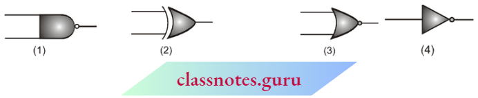
Question 17. Given below are symbols for some logic gates

The XOR gate and NOR gate respectively are
- 1 and 2
- 2 and 3
- 3 and 4
- 1 and 4
Answer: 2. 2 and 3
Question 18. The following truth table corresponds to the logic gate
- A 0 0 1 1
- B 0 1 0 1
- X 0 1 1 1
- NAND
- OR
- AND
- XOR
Answer: 2. OR
Question 19. A truth table is given below. Which of the following has this type of truth table
- A 0 1 0 1
- B 0 0 1 1
- y 1 0 0 0
- XOR gate
- NOR gate
- AND gate
- OR gate
Answer: 2. AND gate
Question 20. An AND gate can be prepared by repetitive use of
- NOT gate
- OR gate
- NAND gate
- NOR gate
Answer: 4. NOR gate
Solids and Semiconductor Devices NEET Physics Class 12 MCQs
Chapter 6 Solids And Semiconductors Devices Multiple Choice Questions Exercise 2
Question 1. For a given circuit potential difference VAB is-

- 10V
- 20V
- 30V
- None
Answer: 1. 10V
Question 2. The resistance of a discharge tube is:
- Zero
- Ohmic
- Non-ohmic
- Infinity
Answer: 3. Non-ohmic
Question 3. For a transistor \(\frac{I_c}{I_E}=0.96\) then current gain for common emitter configuration:
- 12
- 6
- 48
- 24
Answer: 4. 24
Question 4. For the given circuit of the P-N junction diode, which is correct

- In F.B. the voltage across R is V
- In R.B. the voltage across R is V
- In F.B. the voltage across R is 2 V
- In R.B. the voltage across R is 2 V
Answer: 1. In F.B. the voltage across R is V
Question 5. A sinusoidal voltage of peak-to-peak value of 310 V is connected in series with a diode and a load resistance R so that Half-wave rectification occurs. If the diode has negligible forward resistance, the root mean square voltage across the load resistance is
- 310 V
- 155 V
- 109.5 V
- 77.5
Answer: 4. 77.5
Question 6. A photocell employs the photoelectric effect to convert
- Change in the frequency of light into a change in electric voltage
- Change in the intensity of illumination into a change in photoelectric current
- Change in the intensity of illumination into a change in the work function of the photocathode
- Change in the frequency of light into a change in the electric current
Answer: 2. Change in the intensity of illumination into a change in photoelectric current
Question 7. Semiconductor Ge has a forbidden gap of 1.43 eV. Calculate the maximum wavelength that results from the electron-hole combination.
- 8654 Å
- 7650 Å
- 4982 Å
- 10500 Å
Answer: 1. 8654 Å
Question 8. 1. For a given transistor circuit, the base current is 10 A and the collector current is 5.2 mA. Can this transistor circuit be used as an amplifier? Your answer must be supported with a proper explanation.

Answer: yes, \(\beta=520\)
2. For a common emitter amplifier, the current gain is 69. If the emitter current is 7 mA then calculate the base current and collector current.
Answer: \(i_b=0.1 \mathrm{~mA}, \mathrm{i}_{\mathrm{c}}=6.9 \mathrm{Ma}\)
NEET Physics Class 12 Chapter 6 Solids and Semiconductor Devices Question Bank
Chapter 6 Solids And Semiconductors Devices Multiple Choice Questions Exercise 3 Part – 1: Neet Or Aipmt Question (Previous Years)
Question 1. A p-n photodiode is fabricated from a semiconductor with a band gap of 2.5 eV. It can detect a signal of wavelength
- 6000 Å
- 4000 nm
- 6000 nm
- 4000 Å
Answer: 4. 4000 Å
Question 2. The symbolic representation of four logic gates

The logic symbols for OR, NOT, and NAND gates are respectively
- (1) (3), (4), (2)
- (2) (4), (1), (3)
- (3) (4), (2), (1)
- (4) (1), (3), (4)
Answer: 3. (3) (4), (2), (1)
Question 3.
- Draw the circuit diagram of the reversed bias p-n junction.
- Draw the output waveform across the diode in the given circuit.

3. Draw the truth table for the given logic gate.

Question 4. Which one of the following statements is false?
- Pure Si doped with trivalent impurities gives a p-type semiconductor.
- The majority of carriers in a n-type semiconductor are holes.
- Minority carriers in a p-type semiconductor are electrons.
- The resistance of intrinsic semiconductors decreases with an increase in temperature.
Answer: 2. Majority of carriers in a n-type semiconductor are holes.
Question 5. The device that acts as a complete electronic circuit is
- Junction diode
- Integrated circuit
- Junction transistor
- Zener diode
Answer: 2. Integrated circuit
Question 6. A common emitter amplifier has a voltage gain of 50, an input impedance of 100, and an output impedance of 200. The power gain of the amplifier is
- 500
- 1000
- 1250
- 50
Answer: 3. 1250
Question 7. To get an output Y = 1 from the circuit shown below the input must be

- 0 1 0
- 0 0 1
- 1 0 1
- 1 0 0
Answer: 3. 1 0 1
Question 8. The following figure shows a logic gate circuit with two inputs A and B and the output Y. The voltage waveforms of A, B, and Y are as given.

The logic gate is
- NOR gate
- OR gate
- AND gate
- NAND gate
Answer: 4. NAND gate
Question 9. In the following figure, the diodes which are forward-biased, are:

- (3) only
- (3) and (1)
- (2) and (4)
- (1), (2), and (4)
Answer: 2. (3) and (1)
Question 10. Pure Si at 500K has an equal number of electron (n e) and hole (NH) concentrations of 1.5 × 10¹⁶ m–3. Doping by indium increases n h to 4.5 x 10²² m–3. The doped semiconductor is of:
- n-type with electron concentration n e = 5 × 10²² m–3
- p-type with electron concentration n e = 2.5 ×10¹⁰ m–3
- n-type with electron concentration n e = 2.5 × 10²³ m–3
- p-type having electron concentrations n e = 5 × 10⁹ m–3
Answer: 4. p-type having electron concentrations n e = 5 × 10⁹ m–3
NEET Physics Chapter 6 MCQs on Solids and Semiconductor Devices
Question 11. A Zener diode, having a breakdown voltage equal to 15V, is used in a voltage regulator circuit shown in the figure. The current through the diode is:

- 10 mA
- 15 mA
- 20 mA
- 5 mA
Answer: 4. 5 mA
Question 12. A transistor is operated in a common emitter configuration at VC = 2V such that a change in the base current from 100 μA to 300 μA produces a change in the collector current from 10 mA to 20 mA. The current gain is:
- 50
- 75
- 100
- 25
Answer: 1. 50
Question 13. In forward biasing of the p–n junction:
- The positive terminal of the battery is connected to p–the side and the depletion region becomes thick
- The positive terminal of the battery is connected to n–the side and the depletion region becomes thin
- The positive terminal of the battery is connected to n–the side and the depletion region becomes thick
- The positive terminal of the battery is connected to p–the side and the depletion region becomes thin
Answer: 4. The positive terminal of the battery is connected to p–side and the depletion region becomes thin
Question 14. Symbolic representations of four logic gates are shown as:
Pick out which ones are for AND, NAND, and NOT gates, respectively:
- (1) (2), (3) and (4)
- (2) (3), (2) and (1)
- (3) (3), (3) and (4)
- (4) (2), (4) and (3)
Answer: 4. (4) (2), (4) and (3)
Question 15. If a small amount of pentavalent atoms is added to germanium crystal:
- It becomes a P-type semiconductor
- The antimony becomes an acceptor atom
- There will be more free electrons than holes in the semiconductor
- Its resistance is increased
Answer: 3. There will be more free electrons than holes in the semiconductor
Question 16. Two ideal diodes are connected to a battery as shown in the circuit. The current supplied by the battery is:

- 0.75 A
- Zero
- 0.25 A
- 0.5 A
Answer: 4. 0.5 A
Question 17. In a CE transistor amplifier, the audio signal voltage across the collector resistance of 2k is 2V. If the base resistance is 1k and the current amplification of the transistor is 100, the input signal voltage is:
- 0.1 V
- 1.0 V
- 1 mV
- 10 mV
Answer: 4. 10 mV
Question 18. C and Si both have the same lattice structure, having 4 bonding electrons in each. However, C is an insulator where as Si is intrinsic semiconductor. This is because:
- In the case of C the valence band is not filled at absolute zero temperature.
- In the case of C the conduction band is partly filled even at absolute zero temperature.
- The four bonding electrons in the case of C lie in the second orbit, whereas in the case of Si, they lie in the third.
- The four bonding electrons in the case of C lie in the third orbit, whereas for Si they lie in the fourth orbit.
Answer: 3. The four bonding electrons in the case of C lie in the second orbit, whereas in the case of Si, they lie in the third.
Question 19. Transfer characteristics [output voltage (V 0) vs input voltage (Vi )] for a base-biased transistor in CE configuration are shown in the figure. For using a transistor as a switch, it is used:

- In region 3
- Both in the region (1) and (3)
- In region 2
- In region 1
Answer: 2. Both in regions (1) and (3)
Question 20. The figure shows a logic circuit with two inputs A and B and the output C. The voltage waveforms across A, B, and C are as given. The logic circuit gate is:

- OR gate
- NOR gate
- AND gate
- NAND gate
Answer: 1. OR gate
Question 21. The input resistance of a silicon transistor is 100Ω. Base current is changed by 40 mA which results in a change in collector current by 2 mA. This transistor is used as a common emitter amplifier with a load resistance of 4 KΩ. The voltage gain of the amplifier is:
- 2000
- 3000
- 4000
- 1000
Answer: 1. 2000
Question 22. To get an output Y = 1 in a given circuit which of the following inputs will be correct:

Answer: 2.
Question 23. In a n-type semiconductor, which of the following statement is true:
- Electrons are minority carriers and pentavalent atoms are dopants.
- Holes are minority carriers and pentavalent atoms are dopants.
- Holes are majority carriers and trivalent atoms are dopants.
- Electrons are majority carriers and trivalent atoms are dopants.
Answer: Holes are minority carriers and pentavalent atoms are dopants.
Question 24. In a common emitter (CE) amplifier having a voltage gain of G, the transistor used has a transconductance of 0.03 mho and a current gain of 25. If the above transistor is replaced with another one with a transconductance of 0.02 mho and a current gain of 20, the voltage gain will be:
- 1.5 G
- \(\frac{1}{3} G\)
- \(\frac{5}{4} G\)
- \(\frac{2}{3} G\)
Answer: 4. \(\frac{2}{3} G\)
Question 25. The output(X) of the logic circuit shown in the figure will be:

- \(X=\overline{A \cdot B}\)
- X = A.B
- \(X=\overline{A+B}\)
- \(X=\overline{\bar{A}}, \overline{\bar{B}}\)
Answer: 2. X = A.B
Question 26. The given graph represents the V- I characteristic of a semiconductor device.

Which of the following statements is correct?
- It is a V – I characteristic for solar cells where point A represents open circuit voltage and point B short circuit current.
- It is for a solar cell and points A and B represent open circuit voltage and current, respectively.
- It is for a photodiode and points A and B represent open circuit voltage and current respectively.
- It is for an LED and points A and B represent open circuit voltage and short circuit current, respectively.
Answer: 1. It is a V – I characteristic for solar cells where point A represents open circuit voltage and point B short circuit current.
Question 27. The barrier potential of a p-n junction depends on:
- Type of semiconductor material
- Amount of doping
- Temperature
Which one of the following is correct?
- (1) and (2) only
- (2) only
- (2) and (3) only
- (1), (2), and (3)
Answer: 4. (1), (2) and (3)
Question 28. Which logic gate is represented by the following combination of logic gates?

- NAND
- AND
- NOR
- OR
Answer: 2. AND
Question 29. To get output 1 for the following circuit, the correct choice for the input is:

- A = 1, B = 0, C = 1
- A = 0, B = 1, C = 0
- A = 1, B = 0, C = 0
- A = 1, B = 1, C = 0
Answer: 1. A = 1, B = 0, C = 1
Question 30. Consider the junction diode as ideal. The value of current flowing through AB is:

- 10–3 A
- 0 A
- 10–2 A
- 10–1 A
Answer: 3. 10–2 A
Question 31. An NPN transistor is connected in a common emitter configuration in a given amplifier. A load resistance of 800 is connected in the collector circuit and the voltage drop across it is 0.8 V. If the current amplification factor is 0.96 and the input resistance of the circuit is 192, the voltage gain and the power gain of the amplifier will respectively be:
- 4,3.69
- 4,3.84
- 3.69, 3.84
- 4, 4
Answer: 2. 4,3.84
Question 32. The given electrical network is equivalent to

- AND gate
- OR gate
- NOR gate
- NOT gate
Answer: 3. NOR gate
Question 33. In a common emitter transistor amplifier, the audio signal voltage across the collector is 3V. The resistance of the collector is 3k. If the current gain is 100 and the base resistance is 2k, the voltage and power gain of the amplifier are:
- 200 and 1000
- 15 and 200
- 150 and 15000
- 20 and 2000
Answer: 3. 150 and 15000
Question 34. Which one of the following represents the forward bias diode?

Answer: 1.
Question 35. In the circuit shown in the figure, the input voltage Vi is 20 V, VBE = 0, and VCE = 0. The values of I B, I C and are given by
- IB = 40 IA, IC = 10 mA, β = 250
- IB = 40 IA, IC = 5 mA, β= 125
- IB = 20 IA, IC = 5 mA, β = 250
- IB = 25 IA, IC = 5 mA, β= 200
Answer: 2. IB = 40 IA, IC = 5 mA, β= 125
Question 36. In a p-n junction diode, change in temperature due to heating
- Affects only reverse resistance
- Affects the overall V – I characteristics of p-n junction
- Does not affect the resistance of the p-n junction
- Affects only forward resistance
Answer: 2. Affects the overall V – I characteristics of p-n junction
Question 37. In the combination of the following gates the output Y can be written in terms of inputs A and B as

- \(\overline{A \cdot B}\)
- \(\overline{A+B}\)
- \(\overline{A \cdot B}+A \cdot B\)
- \(\text { A. } \bar{B}+\bar{A} \cdot B\)
Answer: 4. \(\text { A. } \bar{B}+\bar{A} \cdot B\)
Question 38. For a p-type semiconductor, which of the following statements is true?
- Electrons are the majority carriers and pentavalent atoms are the dopants.
- Electrons are the majority carriers and trivalent atoms are the dopants.
- Holes are the majority carriers and trivalent atoms are the dopants.
- Holes are the majority carriers and pentavalent atoms are the dopants.
Answer: 3. Holes are the majority carriers and trivalent atoms are the dopants.
Question 39. The correct Boolean operation represented by the circuit diagram drawn is:

- NOR
- AND
- OR
- NAND
Answer: 4. NAND
Question 40. An LED is constructed from a p-n junction diode using GaAsP. The energy gap is 1.9 eV. The wavelength of the light emitted will be equal to
- 10.4 x 10⁻²⁶ m
- 654 nm
- 654 Å
- 654 x 10–11 m
Answer: 1. NAND
Question 41. The circuit diagram shown here corresponds to the logic gate.

- NOR
- AND
- OR
- NAND
Answer: 4. NAND
Question 42. Out of the following which one is a forward-biased diode?

Answer: 4.
Question 43. A n-p-n transistor is connected in a common emitter configuration (see figure) in which the collector voltage drop across load resistance (800 ) connected to the collector circuit is 0.8 V. The collector current is:
- 2 mA
- 0.1 mA
- 1 mA
- 0.2 Ma
Answer: 3. 1 mA
Question 44. Which of the following gates is called a universal gate?
- OR gate
- AND gate
- NAND gate
- NOT gate
Answer: 3. NAND gate
NEET Physics Solids and Semiconductors Devices Practice MCQs
Question 45. An intrinsic semiconductor is converted into an n-type extrinsic semiconductor by doping it with
- Phosphorous
- Aluminium
- Silver
- Germanium
Answer: 1. Phosphorous
Question 46. The increase in the width of the depletion region in a p-n junction diode is due to:
- Increase in forward current
- Forward bias only
- Reverse bias only
- Both forward bias and reverse bias
Answer: 3. Reverse bias only
Question 47. For transistor action which of the following statements is correct?
- The base region must be very thin and lightly doped.
- Base, emitter, and collector regions should have the same doping concentration
- Base, emitter, and collector regions should have the same size
- Both the emitter junction as well as the collector junction are forward-biased
Answer: 1. The base region must be very thin and lightly doped.
Question 48. The electron concentration in an n-type semiconductor is the same as the hole concentration in a p-type semiconductor. An external field (electric) is applied across each of them. Compare the currents in them
- Current in p-type > current in n-type
- Current in n-type > current in p-type
- No current will flow in p-type, current will only flow in n-type
- Current in n-type = current in p-type
Answer: 2. Current in n-type > current in p-type
Question 49. Consider the following Statements (1) and (2) and identify the correct answer.
- A zener diode is connected in reverse bias when used as a voltage regulator.
- The potential barrier of the p-n junction lies between 0.1 V to 0.3 V
- (1) and (2) both are incorrect
- (1) is correct and (2) is incorrect
- (1) is incorrect but (2) is correct
- (1) and (2) both are correct
Answer: 2. (1) is correct and (2) is incorrect
Chapter 6 Solids And Semiconductors Devices Multiple Choice Questions Part – 2 Aims Question (Previous Years)
Question 1. In the following common emitter configuration, an NPN transistor with a current gain = 100 is used. The output voltage of the amplifier will be

- 10 mV
- 0.1 V
- 1.0 V
- 10 V
Answer: 3. 1.0 V
Question 2. The temperature (T) dependence of the resistivity of a semiconductor is represented by

Answer: 3.
Question 3. Which logic gate is represented by the following combination of logic gates?

- OR
- NAND
- AND
- NOR
Answer: 3. AND
Question 4. A transistor connected at common emitter mode contains a load resistance of 5 k and an input resistance of 1 k. If the input peak voltage is 5 mV and the current gain is 50, find the voltage gain.
- 250
- 500
- 125
- 50
Answer: 1. 250
Part – 3: Jee (Main) Or Aieee Problems (Previous Years)
Question 1. The logic circuit shown below has the input waveforms ‘A’ and ‘B’ as shown. Pick out the correct output waveform.

Answer: 4.
Question 2. A p-n junction (D) shown in the figure can act as a rectifier. An alternating current source (V) is connected to the circuit.


Answer: 2.
Question 3. The output of an OR gate is connected to both the inputs of a NAND gate. The combination will serve as a:
- NOT gate
- NOR gate
- AND gate
- OR gate
Answer: 2. NOR gate
Question 4. The truth table for a system of four NAND gates as shown in the figure is:

Answer: 1.
NEET Physics Class 12 Chapter 6 Solids and Semiconductor Devices MCQs
Question 5. The forward-biased diode connection is

Answer: 1.
Question 6. The temperature dependence of resistances of Cu and undoped Si in the temperature range 300 – 400 K, is best described by:
- Linear increase for Cu, exponential increase for Si
- Linear increase for Cu, exponential decrease for Si
- Linear decrease for Cu, linear decrease for Si
- Linear increase for Cu, linear increase for Si
Answer: 2. Linear increase for Cu, exponential decrease for Si
Question 7. If a,b,c,d are inputs to a gate and x is its output, then, as per the following time graph, the gate is:
- AND
- OR
- NAND
- NOT
Answer: 2. OR
Question 8. Identify the semiconductor devices whose characteristics are given below, in the order (1),(2),(3),(4)

- Zener diode, simple diode, Light dependent resistance, Solar cell
- Solar cell, Light dependent resistance, Zener diode, simple diode
- Zener diode, Solar cell, Simple diode, Light dependent resistance
- Simple diode, Zener diode, Solar cell, Light dependent resistance.
Answer: 4. Simple diode, Zener diode, Solar cell, Light-dependent resistance.
Question 9. For a common emitter configuration, if α and β have their usual meanings, the incorrect relationship between α and β is.
- \(\alpha=\frac{\beta}{1-\beta}\)
- \(\alpha=\frac{\beta}{1+\beta}\)
- \(\alpha=\frac{\beta^2}{1+\beta^2}\)
- \(\frac{1}{\alpha}=\frac{1}{\beta}+1\)
Answer: 1.
- \(\alpha=\frac{\beta}{1-\beta}\)
- \(\alpha=\frac{\beta^2}{1+\beta^2}\)
Question 10. In a common emitter amplifier circuit using an n-p-n transistor, the phase difference between the input and the output voltages will be:
- 180°
- 45°
- 90°
- 135°
Answer: 1. 180°
Question 11. The reading of the ammeter for a silicon diode in the given circuit is:
- 11.5mA
- 13.5 mA
- 0
- 15 mA
Answer: 1. 11.5mA
Question 12. The mobility of electrons in a semiconductor is defined as the ratio of their drift velocity to the applied electric field. If, for an n-type semiconductor, the density of electrons is 1019 m-3 and their mobility is 1.6 m2/(V.s) then the resistivity of the semiconductor (since it is an n-type semiconductor (since it is an n-type semiconductor contribution of holes is ignored) is close to:
- 4Ωm
- 0.4Ωm
- 0.2Ωm
- 2Ωm
Answer: 2. 0.4Ωm
Question 13. Ge and Si diodes start conducting at 0.3 V and 0.7 V respectively. In the following figure if the Ge diode connection is reversed, the value of V0 changes by: (assume that the Ge diode has a large breakdown voltage)
- 0.6 V
- 0.2 V
- 0.4 V
- 0.8 V
Answer: 3. 0.4 V
Question 14. To get output ‘1’ at R, for the given logic gate circuit the input values must be:
- X = 1, Y = 1
- X = 0, Y = 0
- X = 0, Y = 1
- X = 1, Y = 0
Answer: 4. X = 1, Y = 0
Question 15. For the circuit shown below, the current through the Zener diode is:
- 14 mA
- 9 mA
- Zero
- 5 mA
Answer: 2. 9 mA
Question 16. The circuit shown below contains two ideal diodes, each with a forward resistance of 50Ω. If the battery voltage is 6 V, the current through the 100Ω resistance (in Amperes) is:

- 0.020
- 0.030
- 0.027
- 0.036
Answer: 1. 0.020
Question 17. In the given circuit the current through the Zener Diode is close to:

- 0.0 mA
- 6.7 mA
- 6.0 mA
- 4.0 mA
Answer: 1. 0.0 mA
NEET Physics Class 12 Chapter 6 Solids and Semiconductor Devices MCQs
Question 18. In the figure, given that supply can vary from 0 to 5.0 V, VCC= 5V,βdc= 200, RB= 100 kΩ, RC= 1 kΩ, and VBE= 1.0 V. The minimum base current and the input voltage at which the transistor will go to saturation will be, respectively:

- 25μA and 2.8 V
- 20μA and 3.5 V
- 20μA and 2.8 V
- 25μA and 3.5 V
Answer: 4. 25μA and 3.5 V
Question 19. The output ofthe given logic circuit is:

- \(A \bar{B}+\bar{A} B\)
- \(\overline{\mathrm{A}} \mathrm{B}\)
- \(A \bar{B}\)
- \(\mathrm{AB}+\overline{\mathrm{AB}}\)
Answer: 3. \(A \bar{B}\)
Chapter 6 Solids And Semiconductors Devices Multiple Choice Questions Self Practice Paper
Question 1. In the circuit shown in the figure, A.C. of peak value 200 volts is being rectified. As compared to the resistance R, the diode resistance is negligible, the r.m.s. value of potential across the R in volts will be approximately_____

- 200
- 100
- \(\frac{200}{\sqrt{2}}\)
- 280
Answer: 2. 100
Question 2. A semiconductor X is made by doping a germanium crystal with arsenic (Z = 33). A second semiconductor Y is made by doping germanium with indium (Z = 49). The two are joined end to end and connected to a battery as shown. Which of the following statements is correct_____

- X is p-type, Y is n-type and the junction is forward biased.
- X is n-type, Y is p-type and the junction is forward biased.
- X is p-type, Y is n-type and the junction is reverse-biased.
- X is n-type, Y is p-type and the junction is reverse-biased.
Answer: 4. X is n-type, Y is p-type, and the junction is reverse-biased.
NEET Physics Class 12 Chapter 6 Solids and Semiconductor Devices MCQs
Question 3. In the following figure, a battery of 2 volts is connected between A and B. It is assumed that the resistance of a diode is zero in forward bias and infinite in reverse bias. If the positive terminal of the battery is connected to A, then the current flowing in the circuit will be________

- 0.1 A
- 0.2 A
- 0.3 A
- Zero
Answer: 2. 0.2 A
Question 4. The reverse current in a P- N junction diode at low reverse voltage is 25µA. The value of forward current at a forward voltage of 0.05 V will be if \(\frac{K T}{e}=0.025\) Volt_______
- 16 mA
- 1.6 mA
- 0.16 mA
- 160 mA
Answer: 3. 0.16 mA